
Comprehensive Analog Front-End (AFE) Engineering: Topology Comparison, Linearity Optimization, and ADC Drive Considerations
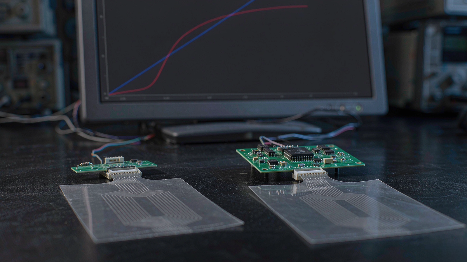 Engineering illustration · FSRTEK technical reference
1. Fundamental Transduction Physics & Conductance Equivalence
Understanding FSR circuit design begins with the physical interface between the carbon-polymer conductive layer and the micro-textured interdigitated electrodes. Under applied mechanical force $F$, micro-asperity contact area increases and quantum tunneling pathways multiply, yielding an approximate power-law transfer function:
$$R_{FSR} approx frac{K}{F^gamma} quad (gamma approx 0.7 sim 1.0)$$
Because resistance is hyperbolic with respect to force, measuring resistance yields severe compression at high loads. Conversely, the conductance $G_{FSR} = frac{1}{R_{FSR}}$ exhibits a substantially linear relationship with applied force across the primary working range:
$$G_{FSR} propto F$$
This physical principle governs the fundamental choice between voltage divider and transimpedance topologies.
2. Voltage Divider Topology: Design Equations & Dynamic Range
The voltage divider is the simplest conditioning interface, ideal for battery-operated edge nodes, keypress thresholds, and binary contact triggers.
Circuit Configuration & Transfer Function
Configured in a high-side FSR arrangement with pull-down reference resistor $R_{ref}$ and clean analog excitation $V_{cc}$:
$$V_{out} = V_{cc} cdot frac{R_{ref}}{R_{FSR} + R_{ref}}$$
Optimal $R_{ref}$ Selection Rule
The maximum voltage sensitivity $frac{dV_{out}}{dF}$ occurs where $R_{ref}$ matches the characteristic mid-range resistance of the FSR under target operating force $F_{mid}$:
$$R_{ref} approx R_{FSR}(F_{mid})$$
- Light Touch Detection (10g ~ 100g): $R_{FSR}$ ranges from $50,text{k}Omega$ to $500,text{k}Omega$; choose $R_{ref} = 47,text{k}Omega sim 100,text{k}Omega$.
- High Force Range (1kg ~ 10kg): $R_{FSR}$ drops to $1,text{k}Omega sim 5,text{k}Omega$; choose $R_{ref} = 2.2,text{k}Omega sim 4.7,text{k}Omega$.
Limitation: The transfer curve exhibits S-shaped non-linearity; sensitivity drops sharply once $R_{FSR} ll R_{ref}$ or $R_{FSR} gg R_{ref}$.
3. Transimpedance (Current-to-Voltage) Op-Amp Topology
For quantitative analog force measurements, tactile grip regulation, and linear calibration, a transimpedance operational amplifier (I-to-V converter) is strongly recommended.
Linearized Transfer Equation
Exciting the FSR with a stable precision reference voltage $V_{ref}$ into the inverting summing junction ($V_- approx 0text{V}$ virtual ground):
$$V_{out} = -V_{ref} cdot frac{R_{f}}{R_{FSR}} = -V_{ref} cdot R_f cdot G_{FSR}$$
Because $V_{out}$ is strictly proportional to conductance $G_{FSR}$, the output voltage scales linearly with applied mechanical force across the linear conductance band, eliminating downstream polynomial linearization overhead.
4. Topology Comparison & Engineering Trade-Off Matrix
| Engineering Parameter | Voltage Divider (Passive + Buffer) | Transimpedance Op-Amp (Active I-to-V) |
|---|---|---|
| Output Linearity | Non-linear (S-curve compression at extremes) | Highly linear with force ($V_{out} propto G_{FSR}$) |
| Circuit Complexity & BOM | Minimal (1 resistor + optional RC filter) | Moderate (Precision Rail-to-Rail Op-Amp + Feedback Network) |
| Dynamic Force Range | 1.5 ~ 2 decades per fixed $R_{ref}$ | 3 ~ 4 decades (adjustable via dynamic gain switching) |
| Input Impedance / Loading | Varies with load; requires high-Z ADC input | Virtual ground input; zero loading effect on sensor |
| Power Consumption | Microamp-level (ideal for coin-cell IoT) | Determined by Op-Amp quiescent current ($50,mutext{A} sim 1,text{mA}$) |
| Recommended Applications | Touch switches, presence detection, battery wearables | Tactile robotics, pressure mapping, precision calibration |
5. Critical Hardware Guidelines for Production PCBAs
- Rail-to-Rail I/O Op-Amps: Select low-offset, low input bias current ($I_b 1,text{M}Omega$.
- ADC Input Drive & RC Antialiasing: Place a low-pass filter ($R = 1,text{k}Omega$, $C = 10,text{nF} sim 100,text{nF}$) immediately adjacent to the MCU ADC input pin to suppress high-frequency mechanical vibration and charge-injection spikes.
- Stable Excitation Voltage: Never excite FSR dividers directly from a noisy digital $3.3text{V}$ rail. Utilize a dedicated LDO or precision reference (e.g. REF3030) to preserve signal-to-noise ratio.
Need an Engineering Review?
Share your sensing requirement, drawing or application target with the FSRTEK team.
Contact Application Engineers